

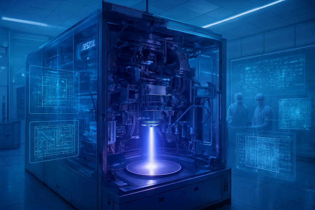
As of February 2026, the global semiconductor industry has officially crossed the threshold into the "Angstrom Era," a pivotal transition marked by the first high-volume shipments of ASML Holding N.V. (NASDAQ: ASML) Twinscan EXE:5200 High-NA EUV lithography systems. These massive, $350 million machines—roughly the size of a double-decker bus—represent the pinnacle of human engineering and are now being deployed at scale by Intel Corporation (NASDAQ: INTC) and Samsung Electronics (KRX: 005930). This milestone signals the end of the experimental phase for High-NA (High Numerical Aperture) technology and the beginning of its role as the primary engine for sub-2nm transistor scaling.
The immediate significance of this development cannot be overstated: for the first time in nearly a decade, the physical limits of standard Extreme Ultraviolet (EUV) lithography are being bypassed. While the industry has relied on 0.33 NA systems to reach the 3nm and 2nm nodes, those systems require "multi-patterning"—essentially printing a single layer multiple times—to achieve the density required for smaller features. With the arrival of High-NA tools, chipmakers can return to "single-exposure" patterning for the most critical layers of a chip, drastically improving yield and performance for the next generation of AI accelerators and high-performance computing (HPC) processors.
The technical leap from standard EUV to High-NA EUV revolves around a fundamental change in the system’s optical physics. While standard EUV systems utilize a numerical aperture (NA) of 0.33, the new Twinscan EXE series increases this to 0.55. This 66% increase in NA allows the system to achieve a resolution of approximately 8nm, a significant improvement over the 13.5nm limit of previous generations. To achieve this, ASML and its partner ZEISS developed a specialized "anamorphic" lens system that magnifies the image differently in the X and Y directions, ensuring that the ultra-fine patterns can still be projected onto a standard-sized silicon wafer without losing fidelity.
The Twinscan EXE:5200B, the current high-volume manufacturing (HVM) standard as of early 2026, is capable of processing between 175 and 200 wafers per hour. This throughput is a critical jump from the initial EXE:5000 R&D models, making it economically viable for mass production. Experts in the lithography community have lauded the machine’s ability to print features at a 1.7x reduction in size compared to its predecessors, resulting in a nearly 2.9x increase in transistor density. This level of precision is mandatory for the fabrication of "Gate-All-Around" (GAA) transistors at the 1.4nm and 1.2nm nodes, where even a few atoms of misalignment can render a chip non-functional.
The rollout of High-NA EUV has created a clear divide in the competitive strategies of the world's leading chipmakers. Intel has taken the most aggressive stance, positioning itself as the "lead customer" and the first to receive both the R&D and HVM versions of the machines. By integrating High-NA into its Intel 14A (1.4nm) process node, the company is betting that it can reclaim the crown of process leadership it lost years ago. Intel CEO Pat Gelsinger has famously referred to these machines as the key to "regaining Moore's Law leadership," aiming to attract major AI clients like NVIDIA (NASDAQ: NVDA) and Amazon (NASDAQ: AMZN) to its foundry services.
Samsung, meanwhile, is pursuing a "fast follower" strategy. After receiving its first production-grade EXE:5200B in late 2025, the South Korean giant is fast-tracking the tech for its SF2 (2nm) and upcoming 1.4nm nodes. Samsung is also looking to apply High-NA to its vertical channel transistor (VCT) DRAM, which is essential for the high-bandwidth memory (HBM4) used in AI data centers. Conversely, Taiwan Semiconductor Manufacturing Co. (NYSE: TSM) has remained more conservative, opting to extend the life of 0.33 NA tools through advanced multi-patterning for its early 1.6nm (A16) node. TSMC’s strategy focuses on cost-efficiency for high-volume customers like Apple (NASDAQ: AAPL), but the company is expected to pivot heavily to High-NA by late 2027 to stay competitive with Intel's aggressive 14A roadmap.
The wider significance of High-NA EUV lies in its role as the critical infrastructure for the global AI boom. To meet the insatiable demand for more powerful Large Language Models (LLMs), AI hardware must provide double-digit improvements in performance-per-watt with every new generation. High-NA EUV is the only technology that permits the transistor density required to pack hundreds of billions of transistors into a single GPU or AI accelerator. Without this technology, the industry would face a "scaling wall," where the power consumption of AI data centers would become unsustainable.
However, the cost of this advancement is staggering. At over $350 million per unit—and with a single fab requiring a fleet of dozens—the barrier to entry for advanced chipmaking is now so high that only the wealthiest nations and corporations can participate. This has turned High-NA tools into instruments of "technological sovereignty." In early 2026, the arrival of these tools at Japan's Rapidus and several US-based facilities highlights a shift toward regionalized, secure supply chains for the world's most critical technology. The environmental impact is also a growing concern, as these massive machines require up to 150 megawatts of power per facility, necessitating a parallel investment in sustainable energy infrastructure.
In the near term, the industry will focus on the "risk production" phase of the 1.4nm node. Intel is expected to begin the first commercial runs for 14A in 2027, with Samsung following closely behind. Beyond 1.4nm, researchers are already looking at "Hyper-NA" lithography, which would push the numerical aperture even higher (potentially beyond 0.75) to reach the 0.7nm and 0.5nm nodes by the early 2030s. Such systems would require entirely new mirror designs and even more extreme vacuum environments.
A significant challenge that remains is the development of the "ecosystem" surrounding the machines. This includes new photoresists (the chemicals that react to the light) and more durable masks that can withstand the intense power of the High-NA light source. Experts predict that the next two years will be defined by a "learning curve" period, during which foundries will work to minimize defects and optimize the "up-time" of these extremely complex systems. If successful, the transition will pave the way for the first trillion-transistor chips before the end of the decade.
The arrival of high-volume High-NA EUV shipments marks one of the most significant milestones in the history of the semiconductor industry. It represents a successful bet against the physics that many thought would end Moore’s Law. For ASML, it solidifies their position as the world's most indispensable tech company. For Intel and Samsung, it is a $350 million-per-unit gamble on the future of computing and their ability to lead the AI-driven world.
As we move through 2026, the industry will be watching for the first "yield reports" from Intel’s 14A and Samsung’s SF2 nodes. These reports will determine whether the massive capital expenditure on High-NA was justified and which company will emerge as the dominant manufacturer for the world's most advanced AI chips. The Angstrom Era is no longer a roadmap item—it is a reality being built, one $350 million machine at a time.
This content is intended for informational purposes only and represents analysis of current AI developments.
TokenRing AI delivers enterprise-grade solutions for multi-agent AI workflow orchestration, AI-powered development tools, and seamless remote collaboration platforms.
For more information, visit https://www.tokenring.ai/.