
Stanford Advanced Materials (SAM) recently announced the launch of its Pyrolytic Boron Nitride (PBN) crucibles with purity as high as 99.99%, helping to address contamination and thermal instability in compound semiconductor crystal growth.
Industry Challenge in Semiconductor Crystal Growth
As semiconductor devices shrink and performance requirements grow increasingly stringent, the demand for ultra-high-purity materials in crystal growth processes has never been greater. Even tiny contamination—like, trace levels—can mess up crystal integrity, hurt electrical properties, and ultimately lower how many good devices you get from production. For manufacturers making compound semiconductors such as gallium arsenide (GaAs) and silicon carbide (SiC), keeping the growth environment squeaky clean is essential. But as production scales up, that's getting harder and harder.
Stanford Advanced Materials (SAM) has launched its high-purity Pyrolytic Boron Nitride (PBN) crucibles for this challenge. These crucibles are designed for outstanding thermal stability and contamination control, giving semiconductor manufacturing a solid, reliable foundation.
PBN Crucibles Designed for High-Purity Crystal Growth
SAM's PBN crucibles are made by chemical vapor deposition (CVD) at high temperature and low pressure, with boron trichloride (BCl₃) and ammonia (NH₃) as the starting materials. This precise manufacturing process gives the crucibles some pretty impressive features:
- Purity of 99.99% or higher, with total impurities under 100 ppm
- Density between 1.95 and 2.22 g/cm³, with a smooth, non-porous surface
- Bending strength around 173 MPa and compression strength of 154 MPa
- Max operating temperature up to 2,400°C—so they can handle even the most extreme heat
- Volume electrical resistivity of 2×10¹⁵ Ω·cm
All these properties make SAM's PBN crucibles chemically inert, highly resistant to thermal shock, and non-wetting to most molten metals and semiconductor materials.
SAM's PBN Crucibles Support Next-Generation Semiconductor Materials
SAM's PBN crucibles help manufacturers lower defect rates, improve crystal uniformity, and boost overall production yield. That directly supports the reliable fabrication of next-gen power electronics, RF devices, and optoelectronic components. SAM's crucibles are suitable for several critical applications:
- Growing compound semiconductor single crystals—such as GaAs, InP, CdTe, and other III–V materials.
- MOCVD and CVD systems for producing semiconductor and optoelectronic epitaxial layers.
- Evaporation crucibles for Molecular Beam Epitaxy (MBE), which is all about ultra-high-vacuum thin-film deposition.
- Evaporation sources for thin-film deposition in vacuum coating systems.
SAM's PBN Crucibles Offer Customization and Flexible Supply
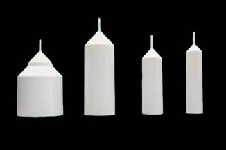
Since crystal growth systems come in all different sizes and designs, SAM offers a wide range of customization options for its PBN crucibles. The product line includes capacities from as small as 5 mL all the way up to 5 liters. SAM can also customize based on drawings.
Stanford Advanced Materials (SAM) also provides several standard configurations, including LEC, MBE, and VGF crucibles, to fit different crystal growth processes. With this kind of flexibility, the products can be tailored to match your specific production needs—helping you get the crucible geometry just right.
About Stanford Advanced Materials
Stanford Advanced Materials (SAM) has been supplying advanced materials for more than 30 years. The new PBN crucible line is simply the latest example of how SAM works to solve real problems for semiconductor manufacturers.
Media Contact
Company Name: Stanford Advanced Materials
Contact Person: Maria Higgins
Email: Send Email
City: Santa Ana
Country: United States
Website: www.samaterials.com