

In semiconductor manufacturing, plasma etching has become a core process for achieving high-precision pattern transfer. However, in mass production environments, the etch uniformity at the wafer edge remains a significant factor affecting yield. Particularly in advanced process nodes where tight etch windows and narrow tolerances are required, non-uniform etching caused by edge effects becomes increasingly prominent. To mitigate this issue, focus rings are widely adopted within etch chambers. This article explores the mechanisms by which focus rings influence etch uniformity at the wafer edge.
1. Origins of Edge Effects
During plasma etching, the wafer is centrally positioned on the electrode or electrostatic chuck, and the process gases flow symmetrically within the chamber. However, due to geometric differences between the wafer edge and chamber wall, localized electric field variations, and gas flow disturbances, the plasma density near the edge often differs significantly from that in the center. This non-uniform plasma distribution leads to higher or lower etch rates at the edge, causing either over-etching or residual defects.
2. Structure and Material Properties of Focus Rings
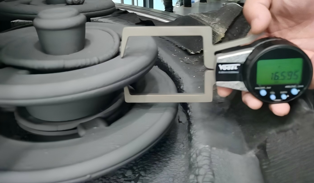
A focus ring is a ring-shaped auxiliary component placed around the wafer edge. It is typically made of ceramic materials similar to those used in the chamber or chuck, such as alumina, quartz, or silicon carbide. Its design must consider dimensional compatibility, electrical insulation, plasma resistance, and thermal stability. By physically extending the wafer edge, the focus ring helps correct plasma distribution during processing.
3. Electric Field Compensation Mechanism
In plasma etching, the sheath electric field generated by RF power determines the energy and trajectory of ion bombardment. At the wafer edge, due to field termination effects, the sheath often bends, causing ions to strike at oblique angles, which leads to non-uniform etching. Focus rings help extend the edge potential profile and suppress sheath bending, forming a smoother electric field contour. This allows ions at the edge to impact the wafer surface more vertically, improving symmetry and consistency of etch profiles.(1)
4. Gas Flow and Reactant Distribution Optimization
Focus rings also regulate the flow path of process gases in the chamber. With appropriate design in terms of height and spacing, the focus ring can reduce turbulence and redirection of gas flow at the wafer edge, ensuring more consistent reactant concentrations between the edge and center. Additionally, it helps minimize by-product redeposition, reducing the occurrence of edge defects.
5. Thermal Uniformity and Material Matching
In terms of thermal management, the thermal conductivity and expansion coefficients of the focus ring must match the wafer support structure. Mismatches can lead to localized stress or etch rate drift due to thermal imbalances. A well-matched thermal field stabilizes the edge temperature, ensuring better control over the chemical reactions involved in etching.
6. Focus Ring Lifetime and Process Stability
Over time, the surface of the focus ring undergoes morphological changes due to ion bombardment and chemical corrosion, potentially reducing its ability to regulate electric fields and gas flow. Therefore, periodic replacement and monitoring of wear levels are critical to maintaining edge uniformity. Advanced processes may even employ adjustable or multi-segment focus rings to further expand process windows and enhance consistency. (2)
As a key auxiliary component within plasma etch chambers, the focus ring plays a multifaceted role in improving edge etch uniformity. Through precise design and maintenance, it enhances pattern consistency and contributes to greater process yield and stability. With the ongoing advancement of semiconductor nodes and their stringent edge control requirements, focus ring designs will continue to evolve, solidifying their importance in next-generation etching equipment.
Author:Semicera
Reference:(1)G. S. Oehrlein et al., “Plasma-surface interactions in advanced etching processes,” IBM Journal of Research and Development, 2005.
(2)Lam Research, “Focus Ring Design for Plasma Etching,” Technical White Paper, 2021.
Media Contact
Company Name: Ningbo Miami Advanced Material Technology Co., LTD
Email: Send Email
Country: China
Website: https://www.semi-cera.com/